- Products & Capabilities

- Simulation Design & EDA

- About
- Resources
PCBX.com Resources
Your source for industry knowledge, news, and expert insights

Latest Posts
Article
BGA rework stations offer precision, automation, and cost-efficiency, solving challenges in high-density electronics by optimizing component alignment and heating.
 2024/12/19
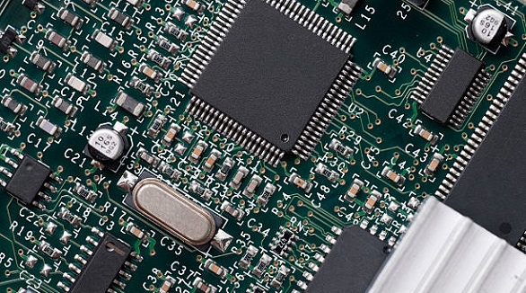
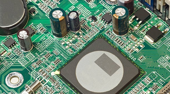
The main PCB is crucial for mounting and connecting electronic components, vital for device performance. It supports design and manufacturing innovations.
2024/12/19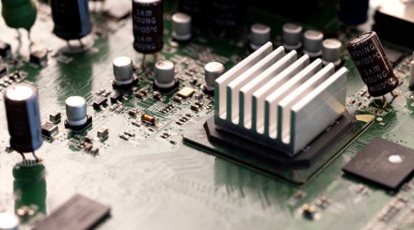
Capacitive circuits store and release energy, stabilize voltage, filter signals, and manage power flow, making them vital for modern electronic systems.
2024/12/11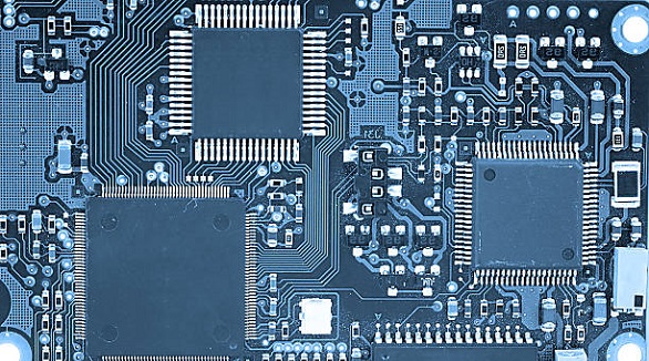
Cold solder joints result from improper soldering, impacting PCB performance. Detection and prevention via proper technique and equipment ensure reliability.
2024/11/26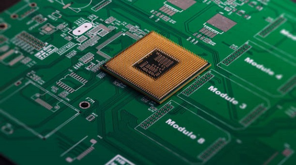
PCB pads connect components on circuit boards. Understanding through-hole, surface-mount, and BGA pads is key for effective PCB design and manufacturing.
2024/11/08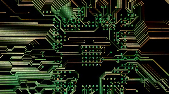
Understanding PCB current ratings ensures safe electric flow. Optimize trace size, copper weight, and use via calculators and high-current connectors for efficient and reliable PCB designs.
2024/10/17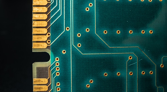
Vias in PCBs connect multiple layers and come in types like through-hole, microvias, blind, and buried. Proper sizing and design optimize PCB performance and reliability, aiding advanced device development.
2024/10/16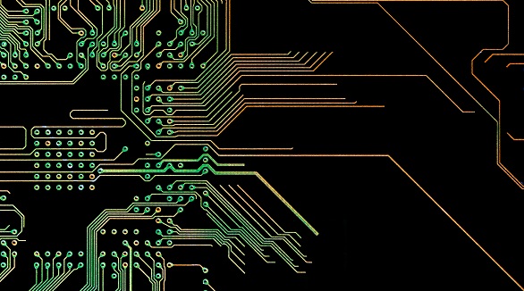
PCB trace technology is crucial for modern electronics, ensuring reliable and efficient signal transmission. Key elements include trace width, spacing, and material selection.
2024/09/25