- Products & Capabilities

- Simulation Design & EDA

- About
- Resources
PCBX.com Resources
Your source for industry knowledge, news, and expert insights

Latest Posts
Article
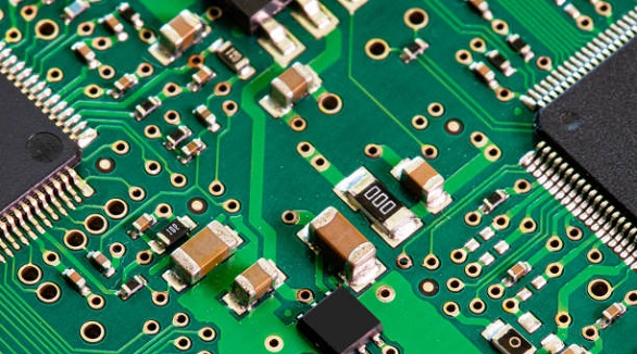
SMT revolutionizes electronics by enabling smaller, efficient, durable devices, with reduced costs and performance boosts, essential in various industries.
 2025/01/24
Populated circuit boards integrate electronic components for efficiency and reliability, utilizing SMT and THT for diverse applications across industries.
2024/12/17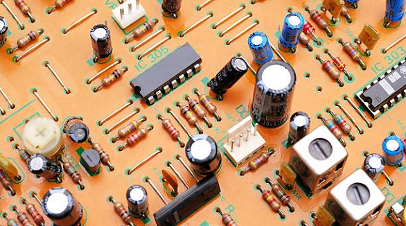
Through-hole assembly remains essential in electronics, offering strength and reliability, especially in critical applications, despite SMT's rise in compact designs.
2024/12/05
PCB pads connect components on circuit boards. Understanding through-hole, surface-mount, and BGA pads is key for effective PCB design and manufacturing.
2024/11/08
BGA packages enhance connectivity but pose rework challenges due to solder ball grids. Effective rework requires specialized tools, precision, and practice for safe removal and replacement.
2024/10/10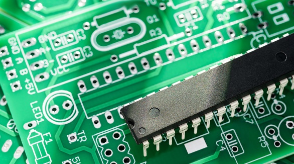
Through-hole technology remains vital in electronics for its reliability and durability. The article reviews its components, benefits, applications, and evolving trends like miniaturization, SMT integration, and automation.
2024/09/27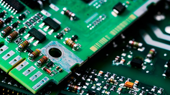
Through-Hole Technology (THT) mounts electronic components by inserting their leads through pre-drilled PCB holes and soldering them. While durable and ideal for harsh conditions, THT is less space-efficient than SMT.
2024/09/16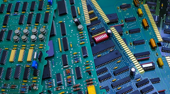
Mixed Assembly PCBs combine Surface Mount Technology (SMT) and Through-Hole Technology (THT) for high-performance, compact, and reliable circuit boards. This integration leverages both technologies to enhance reliability, component selection, flexibility, and efficiency. Used in CPUs, IoT hardware, and more, they offer economic, efficient manufacturing for versatile applications in modern electronics.
2024/09/12