PCBX.com Resources
Your source for industry knowledge, news, and expert insights

Latest Posts
Article
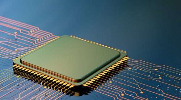
TQFP packages optimize PCB layout with space efficiency, RoHS compliance, and high reliability, addressing die shrinking and enhancing portability.

PCBX's new platform streamlines PCB design, offering real-time simulations, prototyping, and collaboration tools for students, hobbyists, and professionals.
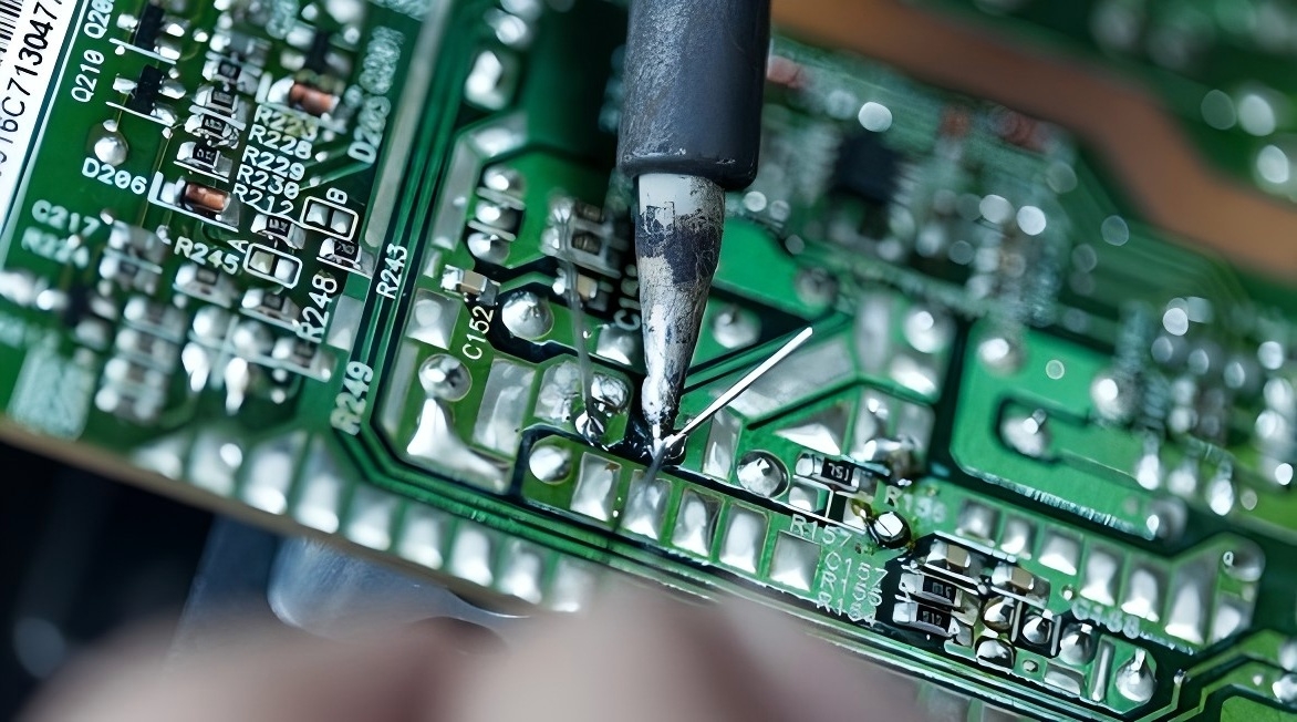
SMD offers stability and control in PCBs, ideal for high-density uses. NSMD provides flexibility and stronger joints, better for mechanical tolerance.
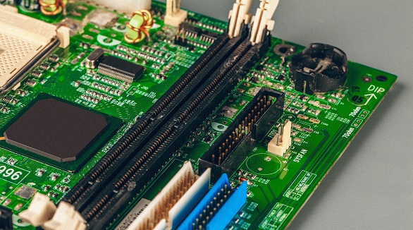
Efficient PCB assembly needs component standardization, design clarity, optimized workflow, material management, defect detection, automation, teamwork, lean practices, and IoT integration to meet quality and demand.
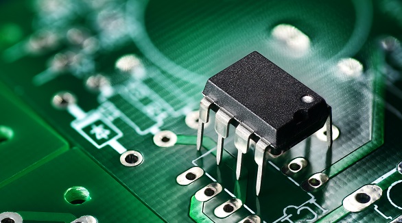
DIP is a basic, cost-effective IC package with dual-row pins, offering ease of use and reliability but taking more PCB space. It's ideal for prototyping and durable applications.
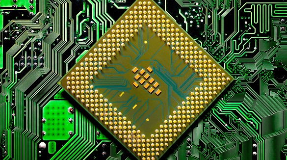
BGA assembly, challenging due to hidden joints and warpage, requires advanced techniques, skilled training, and strategic planning for reliable PCB production and minimized defects.
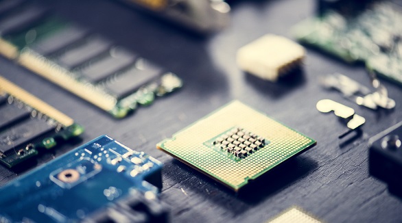
BGA rework is complex, requiring skilled training, quality tools, precise thermal control, and thorough inspections to prevent costly errors and improve PCB assembly efficiency.
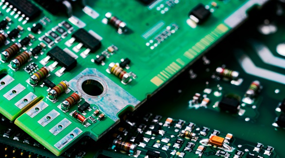
Printed Circuit Board Assembly (PCBA) employs Through-Hole Technology (THT) and Surface Mount Technology (SMT). THT offers robust mechanical bonds, ideal for high-stress applications, whereas SMT supports efficient, high-density assemblies. Each method has unique advantages and limitations, impacting cost, manufacturing efficiency, and component compatibility. Understanding these differences is key for optimal PCB design.
