- Products & Capabilities

- Simulation Design & EDA

- About
- Resources
PCBX.com Resources
Your source for industry knowledge, news, and expert insights

Latest Posts
Article

Pin in Paste (PiP) enables efficient, cost-effective PCB assembly, integrating through-hole and surface mount components in a single reflow pass, reducing costs.
 2025/02/17
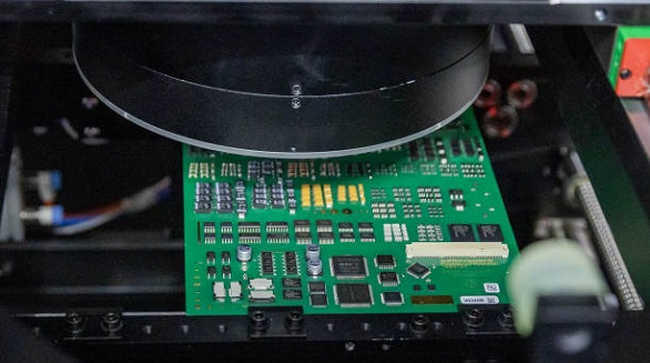
Mastering hot air rework to remove SMD chips ensures precise control, protects the PCB, and is vital for effective electronics repair and upgrades.
2025/01/22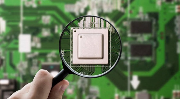
ARM processors are efficient and flexible, ideal for many applications, while FPGAs offer custom parallel processing, crucial for specialized tasks requiring flexibility.
2025/01/21
The 0603 SMD, vital for compact electronics, offers space efficiency, versatility, and cost-effectiveness, crucial for industries like consumer electronics and automotive systems.
2025/01/21
Hex inverter ICs are vital in digital electronics for signal inversion, logic functions, oscillators, and data transmission, enabling efficient circuit designs.
2025/01/20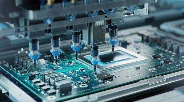
Ensure SMT quality through detailed design, supplier rigor, and process controls, enhanced by testing and continuous improvement for reliable, defect-free products.
2025/01/15
BGAs offer efficient, reliable IC connections with superior performance, comprising seven types ideal for high-performance electronics, optimizing space and thermal efficiency.
2025/01/14
Selecting the right circuit components ensures functionality and reliability by matching specifications like voltage, current, and resistance for optimal performance.
2025/01/14